Demonstrate Basic Electronic Skills
Level 6 — Basic Electronic Skills — July/August 2024 — Written
Source-based revision questions and worked answers for Jemshah learners. These are study answers, not an official CDACC marking scheme. Printed errors and unreadable details are identified in the affected answers.
Question 1
Define the term ‘diode ’as used in basic electronics.
(2 Marks)
Answer
A diode is a two-terminal semiconductor device with a strongly asymmetric current–voltage characteristic: it conducts readily in the forward direction and largely blocks reverse current below breakdown.
Question 2
Explain the meaning of the following terms as used in semiconductors.
a. P–N junction.
(2 Marks)
b. Doping.
(2 Marks)
Answer
a. A P–N junction is the boundary between adjacent p-type and n-type semiconductor regions. Initial diffusion and recombination create a depletion layer and internal electric field. b. Doping is adding a small controlled quantity of donor or acceptor impurities to change a semiconductor’s carrier concentration and conductivity.
Question 3
Elaborate THREE ways in which the use of BCD representation enhances accuracy in
applications.
(3 Marks)
Answer
- Each decimal digit has an exact four-bit representation, so entered decimal digits need not be approximated as binary fractions.
- With a fixed decimal scale, monetary values can be stored as exact decimal quantities, avoiding some binary floating-point rounding issues.
- Decimal digit checking and display conversion are straightforward; invalid digit codes 1010–1111 can be detected. BCD still requires correct arithmetic and does not automatically prevent all errors.
Question 4
Sumo Company is assessing a robust power supply unit, which is rated at 1200W and operates at
220V. Determine the current drawn by the supply unit and calculate its resistance.
(4 Marks)
Answer
Worked calculation
- Assume a resistive load (or the effective resistance of an ideal unity-power-factor load).
- I = P/V = 1200/220 = 5.45 A.
- R = V²/P = 220²/1200 = 40.33 Ω.
Question 5
Enumerate THREE terminals of a transistor.
(3 Marks)
Answer
Emitter, base and collector.
Question 6
Explain TWO characteristics of passive electronic components.
(4 Marks)
Answer
- They cannot produce net power gain: output energy cannot exceed the energy supplied to them.
- They dissipate energy or store and return it, as in resistors, capacitors and inductors.
Question 7
Describe the position of the chemical potential in an n-type semiconductor at room temperature.
(3 Marks)
Answer
The chemical potential (Fermi level) in non-degenerate n-type silicon lies in the band gap closer to the conduction-band edge than in intrinsic silicon. Donor impurities raise the electron concentration and shift the Fermi level upwards. Its exact position depends on doping density and temperature; it is not generally inside the conduction band for ordinary doping.
Question 8
State THREE characteristics of volatile memory.
(3 Marks)
Answer
- Contents are lost when power is removed.
- A continuous power supply is required to retain information.
- It supports rapid read/write working storage. DRAM also needs periodic refresh; SRAM does not require refresh while powered.
Question 9
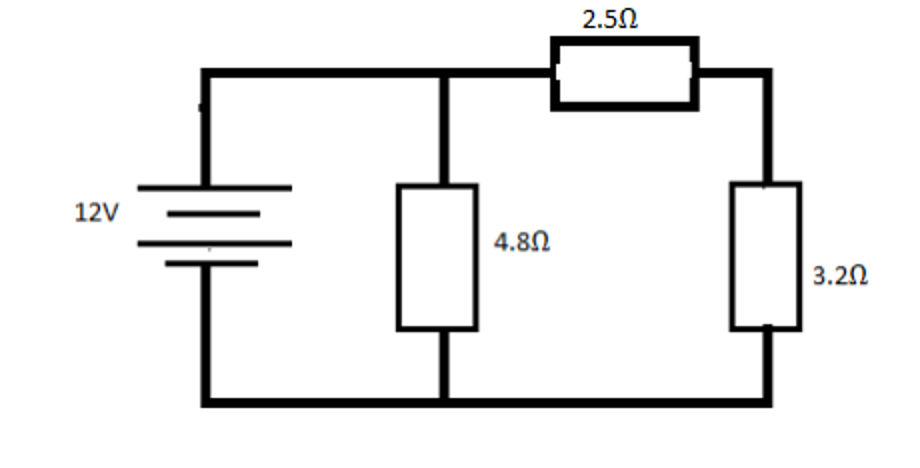
Using the circuit in Figure 1, determine the current passing through it when powered by a 12-volt source. (4 marks)
Answer
Worked calculation
- The 2.5 Ω and 3.2 Ω resistors form a series branch: Rb = 2.5 + 3.2 = 5.7 Ω.
- That branch is in parallel with 4.8 Ω.
- Req = (4.8 × 5.7)/(4.8 + 5.7) = 2.6057 Ω.
- Supply current = 12/2.6057 = 4.6053 A.
- Branch currents: 12/4.8 = 2.5 A and 12/5.7 = 2.1053 A; their sum agrees.
Question 10
Explain the implications of adding a new resistor to a series circuit compared to a parallel circuit
in terms of overall resistance.
(4 Marks)
Answer
In series, Rtotal = R1 + R2 + …, so adding a positive resistance increases total resistance and reduces current at fixed supply voltage. Adding another parallel branch increases total conductance: 1/Rtotal = 1/R1 + 1/R2 + … . Therefore equivalent resistance decreases and supply current increases at fixed voltage.
Question 11
Perform the conversions for each of the following number system.
a. 72010 to Octal.
(3 Marks)
b. 5BC16 to Decimal.
(3 Marks)
Answer
Worked calculation
- 720 ÷ 8 = 90 remainder 0; 90 ÷ 8 = 11 remainder 2; 11 ÷ 8 = 1 remainder 3; 1 ÷ 8 = 0 remainder 1.
- Read remainders backwards: 720₁₀ = 1320₈.
- 5BC₁₆ = 5×16² + 11×16 + 12 = 1280 + 176 + 12 = 1468₁₀.
Question 12
As part of your interview process for a computer scientist position at a software development
company, you're asked to demonstrate your foundational knowledge in electronics by performing
computations in various number systems
a. Perform the conversions for each of the following number system.
(10 Marks)
i.
011110102to Decimal
ii.
0100 0011 0110 0010(BCD) to hexadecimal
iii.
EA5416 to Binary
iv.
61710 to Binary
v.
111110.111100 to Decimal
b. Justify FIVE reasons why silicon is preferred over germanium for semiconductor devices.
(10 Marks)
Answer
a. Conversions
Worked calculation
- i. 01111010₂ = 64 + 32 + 16 + 8 + 2 = 122₁₀.
- ii. 0100 0011 0110 0010 in BCD gives decimal digits 4,3,6,2: 4362₁₀ = 110A₁₆.
- iii. EA54₁₆ = 1110 1010 0101 0100₂ (convert each hexadecimal digit to four bits).
- iv. 617 = 512 + 64 + 32 + 8 + 1, so 617₁₀ = 1001101001₂.
- v. 111110.111100₂ = 62 + 1/2 + 1/4 + 1/8 + 1/16 = 62.9375₁₀.
b. Silicon advantages
- Silicon is abundant and generally cheaper as a raw material.
- Its larger band gap gives lower intrinsic carrier concentration and less leakage at a given temperature.
- It tolerates higher operating temperatures before leakage becomes excessive.
- It forms a stable, useful silicon-dioxide insulating layer, important in integrated-circuit fabrication.
- Its mature processing technology supports reliable, dense, mass-produced integrated circuits.
Question 13
a. Describe FOUR examples of special diodes commonly used in Computer equipment.
(8 Marks)
b. With the help of a diagram, discuss the FOUR main hierarchy of the computer memory.
(12 Marks)
Answer
a. Special diodes
- Zener diode: operated in controlled reverse breakdown for voltage reference or regulation.
- LED: produces light under forward bias for indicators and displays.
- Schottky diode: metal–semiconductor junction with low forward drop and fast switching for rectification.
- Photodiode: converts incident light into current for optical sensing or data reception.
b. Memory hierarchy
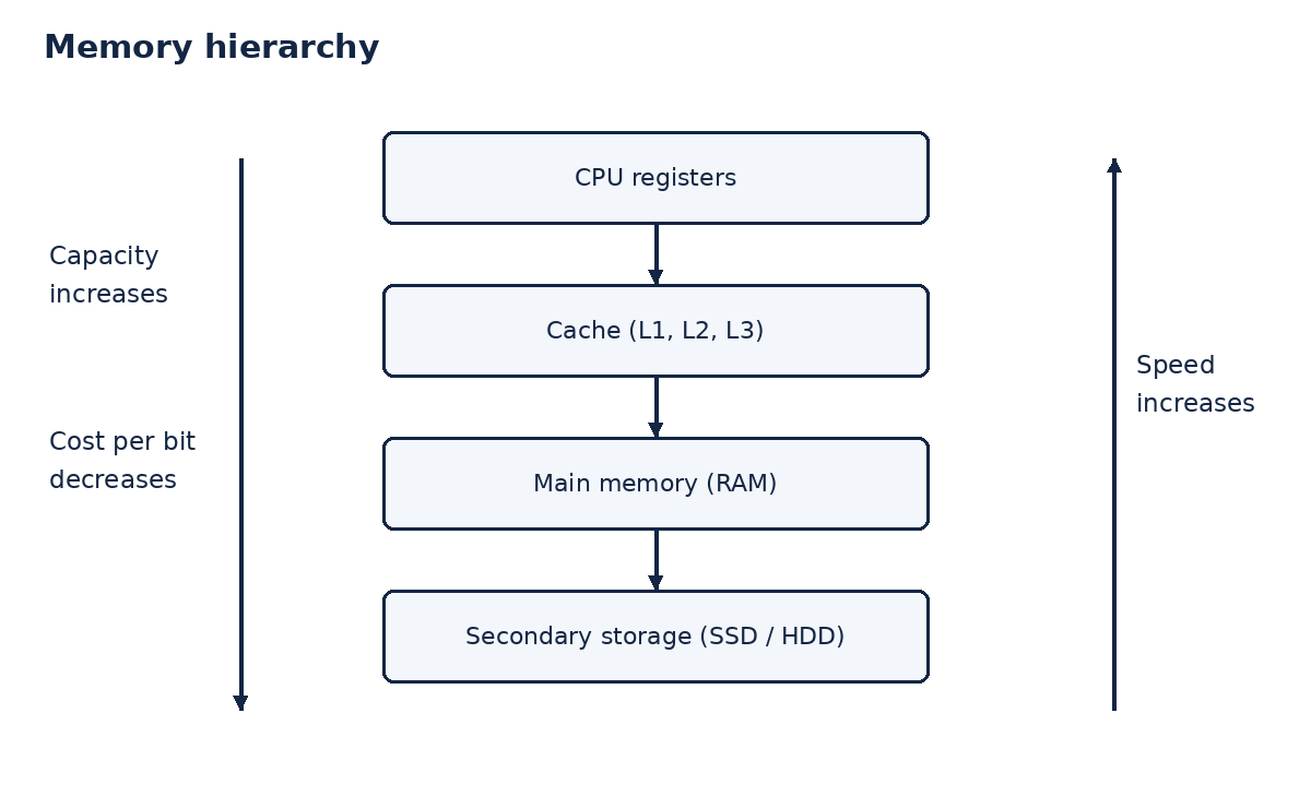
- Registers are inside the CPU and hold current operands and results; they are the smallest and fastest level.
- Cache keeps copies of recently used memory blocks; it is very fast but has limited capacity.
- Main memory (RAM) holds running programs and working data; it is larger and slower than cache.
- Secondary storage (SSD/HDD) retains files without power; it is much larger and has much higher access latency. Moving down the hierarchy normally increases capacity and lowers cost per bit while reducing speed.
Question 14
a. John has been designated to train recently onboarded staff at the Tech Solutions firm
where he is employed. As a component of the training agenda, he is obligated to delve
into the fundamentals of electronics.
i.
Using well-labelled diagrams, describe how a P-N junction diode is biased.
(10 Marks)
ii.
Discuss FIVE applications of PNP transistors.
(10 Marks)
Answer
a(i). Diode bias

Forward bias connects P/anode to positive and N/cathode to negative, through a current-limiting resistor. The external field reduces the barrier and narrows the depletion region; majority carriers cross the junction and appreciable current flows. Reverse bias connects P to negative and N to positive. The barrier rises and the depletion region widens, leaving only small leakage current until breakdown. A diode’s forward voltage is not an exact universal threshold; approximately 0.7 V is a common silicon circuit approximation.
a(ii). PNP applications
- High-side switching: a control circuit switches a load connected below a positive supply.
- Audio amplification: a small base signal controls a larger emitter–collector current.
- Complementary push-pull output stages: a PNP device works with an NPN device to handle opposite portions of a signal.
- Current sources and current mirrors: matched devices supply approximately controlled currents.
- Voltage-regulator or driver circuits: a PNP pass transistor regulates or supplies load current with appropriate bias and protection.
Question 15
a. An electronics technician is in the midst of crafting a new system. As the technician
progresses, she recognizes the crucial considerations involved in selecting the appropriate
semiconductors before defining the circuit requirements.
i.
Discuss FIVE differences between intrinsic and extrinsic semiconductors that will
guide the technician on choosing the best semiconductor to use.
(10 Marks)
b. A 10 Ω and a 4 Ω resistor are connected in series; the current is measured to be 8A.
i.
Draw the diagram for the above circuit.
(4 Marks)
ii.
Compute the voltage drop across the 4 Ω resistor.
(3 Marks)
iii.
Calculate the total power dissipated by the circuit.
(3 Marks)
Answer
a. Semiconductor comparison
| Property | Intrinsic | Extrinsic |
|---|---|---|
| Composition | Pure semiconductor | Doped with controlled impurities |
| Carrier source | Thermally generated electron–hole pairs | Dopants supply majority carriers; thermal pairs also exist |
| Carrier balance | Electron and hole densities equal | Electrons dominate in n-type; holes dominate in p-type |
| Conductivity | Relatively low at a given temperature | Normally higher at the same temperature |
| Fermi level | Near the middle of the band gap | Shifted towards conduction band (n) or valence band (p) |
b. Series circuit

Worked calculation
- i. Rtotal = 10 + 4 = 14 Ω; source voltage = 8 × 14 = 112 V.
- ii. Voltage across 4 Ω = IR = 8 × 4 = 32 V.
- iii. Total power = I²Rtotal = 8² × 14 = 896 W.