Level 6 — Electronic Skills — Jul/Aug 2025
Level 6 • July/August 2025 • Written assessment
Work through each question before checking the answer. These revision answers are prepared for learners; they are not an official marking scheme.
Question 1
Answer
Silicon atoms share four valence electrons in covalent bonds. In a large crystal, interacting atomic energy levels split into closely spaced allowed levels, forming bands. The valence band contains bonding-electron states; the conduction band contains higher-energy states in which electrons can move through the crystal. A forbidden energy gap separates the bands.
Question 2
Answer
At 0 K, ideal intrinsic silicon has a full valence band and an empty conduction band, so there are no thermally generated mobile carriers. At room temperature, some electrons gain sufficient thermal energy to cross the band gap. Each promoted electron leaves a hole in the valence band; both the electrons and holes contribute to conduction. The relatively small semiconductor band gap permits this limited carrier generation.
Question 3
Answer
- Pixels = 1920 × 1080 = 2,073,600.
- Bits = 2,073,600 × 24 = 49,766,400.
- Bytes = 49,766,400 / 8 = 6,220,800.
- Using decimal megabytes: 6,220,800 / 1,000,000 = 6.2208 MB. Using 1,048,576 bytes per MiB gives 5.9326 MiB. This excludes file headers and row padding.
Question 4
Answer
- Total series resistance = 27 + 33 + 56 = 116 Ω.
- Current = V/R = 240/116 = 2.06897 A.
- Voltage across 33 Ω = IR = 2.06897 × 33 = 68.28 V.
Question 5
Answer
- An electron becomes a mobile conduction electron after gaining enough energy to leave a covalent bond and enter the conduction band.
- The missing bonding electron leaves a hole. Nearby valence electrons can fill the hole, making the hole appear to move as a positive charge carrier. Intrinsic generation creates electron–hole pairs.
Question 6
Answer
- Phosphorus.
- Arsenic. Both are pentavalent donor dopants; antimony is another valid example.
Question 7
Answer
R = ρL/A for a uniform conductor. With material, length and temperature held constant, resistance is inversely proportional to area: doubling A halves R.
Question 8
Answer
- Lower access latency for frequently used instructions/data than main RAM.
- Exploits locality to reduce repeated main-memory accesses and processor waiting time.
Question 9
Answer
- The hexadecimal digit B is valid and equals decimal 11.
- Map each hex digit to four bits: 1→0001, 3→0011, 5→0101, 4→0100, B→1011.
- 1354B₁₆ = 0001 0011 0101 0100 1011₂ (leading zeros may be omitted).
- Integer part: 126 ÷ 16 = 7 remainder 14 (E), so 126 = 7E₁₆.
- Fraction: 0.02×16 = 0.32 (digit 0); 0.32×16 = 5.12 (5); 0.12×16 = 1.92 (1); 0.92×16 = 14.72 (E); 0.72×16 = 11.52 (B); 0.52×16 = 8.32 (8).
- The fraction then repeats from 0.32: 126.02₁₀ = 7E.051EB851EB8…₁₆, a non-terminating hexadecimal fraction.
Question 10
Answer
The printed A is invalid: octal digits can only be 0–7, so 18₈ has no defined value. B = 10₂ = 2. A correction is needed before an exact sum can be calculated.
- After a valid correction, convert both operands to decimal and add.
- Encode each decimal digit separately by adding 3 and writing its four-bit binary value.
- Illustration only: if the intended A were 18₁₀, the sum would be 20; 2+3=5→0101 and 0+3=3→0011, giving 0101 0011. This is conditional, not a claimed correction to the paper.
Question 11
Answer
- Available RAM = (8 − 1.5) × 1024 = 6656 MB.
- 6656 / 750 = 8.8747.
- Round down to whole instances: 8 instances. They use 6000 MB; 9 would use 6750 MB, exceeding 6656 MB.
Question 12
Answer

- Parallel resistance = (27×56)/(27+56) = 1512/83 = 18.2169 Ω.
- Total = 82 + 47 + 18.2169 = 147.2169 Ω.
- Supply current = 230/147.2169 = 1.562 A.
- Forward diode current = (5 − 0.7)/1000 = 0.0043 A = 4.3 mA.
- With the diode reversed at 5 V, current is approximately zero in the ideal model; a real diode has small leakage, assuming reverse breakdown is not reached.
- 001110₂ × 011100₂ = 14×28 = 392 = 110001000₂.
- 0011011.011₂ + 001100.111₂ = 27.375 + 12.875 = 40.25 = 101000.010₂.
- PROM: programmed once to hold permanent instructions/data.
- EPROM: can be erased with ultraviolet light and reprogrammed.
- EEPROM/flash: non-volatile memory that can be electrically erased and rewritten; flash normally erases blocks.
Question 13
Answer
| Material | Conductivity |
|---|---|
| Silver | Excellent metal conductor with many mobile electrons |
| Silicon | Semiconductor; conductivity depends strongly on doping and temperature |
| Glass | Electrical insulator under ordinary conditions; very few mobile carriers |
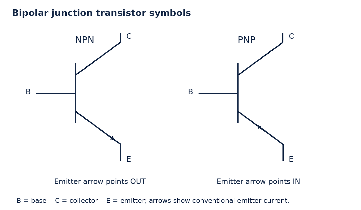
An NPN transistor has n-type emitter and collector separated by a thin p-type base; in forward-active operation, conventional collector current enters the collector and leaves through the emitter. A PNP reverses the conductivity types and current/voltage polarities; the emitter arrow points toward the base. For either type, IE = IC + IB.
- Power = VI = 440 × 4 = 1760 W.
- Excess-3: 6→1001 and 5→1000. Add: 1001 + 1000 = 1 0001.
- There is a decimal carry; correct the remaining nibble by adding 0011: 0001 + 0011 = 0100 (Excess-3 for decimal 1).
- The tens digit is also decimal 1, encoded 0100. Result for 11 = 0100 0100.
Question 14
Answer
| Observation | Interpretation |
|---|---|
| No base current and no collector current | Cutoff: the transistor is off (apart from leakage) |
| Maximum circuit-limited collector current | Saturation: the transistor acts as an on switch; both junctions are forward biased |
- Non-volatile: keeps firmware without power.
- Provides stable startup instructions before general applications load.
- Protects against accidental changes; update protection depends on the ROM technology.
- Provides reliable repeated reading with little routine write activity.
The 1500 W value is legible in the original copy; it was obscured in the edited scan.
- Current = P/V = 1500/220 = 6.82 A.
- Power = 1.5 kW; 10 minutes = 10/60 hour. Energy = 1.5×10/60 = 0.25 kWh.
- For 45 minutes: energy = 1.5×45/60 = 1.125 kWh.
- Cost = 1.125×29 = KSh 32.625 ≈ KSh 32.63.
Question 15
Answer
- Use integrated components to reduce size and assembly cost.
- Design efficient power electronics and low-power operating modes.
- Use lightweight durable materials for portability.
- Improve useful features and ergonomics based on customer feedback.
- Offer reliable quality, competitive pricing and repair/support options.
- Convert spacing: d = 2 mm = 0.002 m.
- For a vacuum parallel-plate capacitor, C = ε₀A/d.
- C = (8.85×10⁻¹²×0.5)/0.002 = 2.2125×10⁻⁹ F = 2.2125 nF.
- Moving parts are vulnerable to shock and mechanical failure.
- Random access is slower than typical solid-state storage.
- A removable drive can be lost, stolen or disconnected; protect data with encryption and backups.
- Write each digit separately: 454 = 0100 0101 0100; 234 = 0010 0011 0100.
- Add units: 0100 + 0100 = 1000 (8), a valid BCD digit.
- Add tens: 0101 + 0011 = 1000 (8), a valid BCD digit.
- Add hundreds: 0100 + 0010 = 0110 (6), a valid BCD digit.
- Result = 0110 1000 1000 (BCD) = 688₁₀. No digit needs the +0110 BCD correction in this addition.