Module I — Computer Architecture — Nov/Dec 2025
Module I • Level not stated • November/December 2025 • Written assessment
Work through each question before checking the answer. These revision answers are prepared for learners; they are not an official marking scheme.
Question 1
Answer
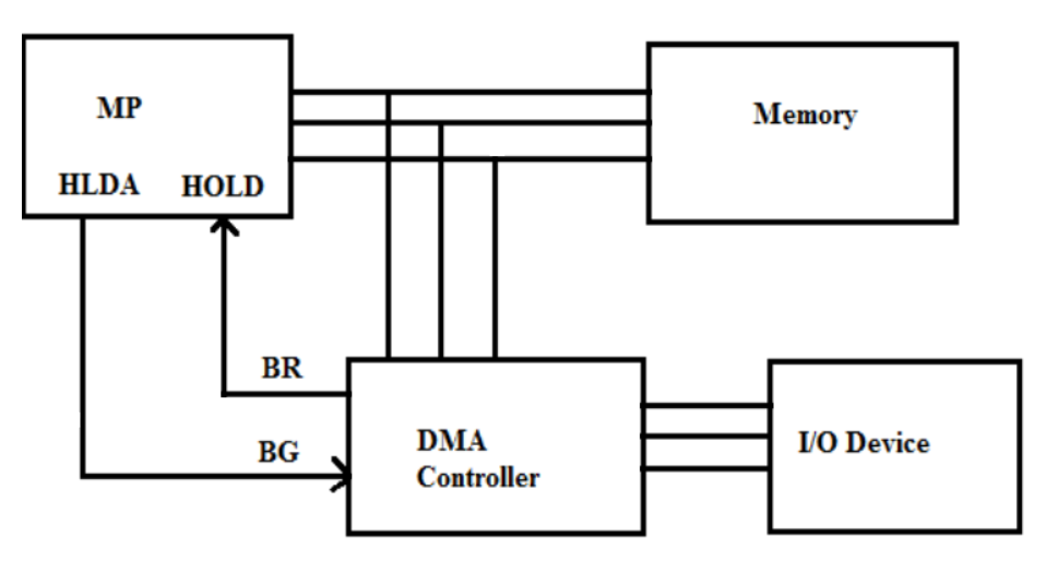
- The CPU programs the DMA controller with the memory address, transfer count and direction.
- The controller requests the bus using HOLD/bus request.
- The CPU finishes its current bus transaction and acknowledges with HLDA/bus grant.
- The controller transfers data between the device and memory, updates the address/count, releases the bus and signals completion.
Question 2
Answer
- Their capacity is small compared with modern solid-state and disk storage.
- Mechanical optical reading/writing is comparatively slow.
- Discs scratch or deteriorate and require a separate optical drive.
- Flash drives, network storage and online transfer are convenient and widely supported.
Question 3
Answer
| Device | Classification |
|---|---|
| Digitizer | Input |
| Page scanner | Input |
| Light pen | Input |
| Projector | Output |
Question 4
Answer
- Replace each hexadecimal digit by four bits: F = 1111, A = 1010, D = 1101, 5 = 0101.
- FAD5₁₆ = 1111101011010101₂.
- Group the binary number from the right: 111 101 001 011.
- The groups are 7, 5, 1, 3, so 111101001011₂ = 7513₈.
Question 5
Answer
A flash drive used to accelerate an older Windows system refers to ReadyBoost, a storage cache, rather than virtual-machine creation or additional physical RAM. The wording is imprecise.
- Insert a compatible flash drive into a computer/version of Windows that supports ReadyBoost.
- Open File Explorer, right-click that drive and open Properties.
- Choose the ReadyBoost tab; select “Use this device” or dedicate it to ReadyBoost if the system accepts the device.
- Choose the cache space and apply the settings. If Windows says the computer/device is unsuitable, do not force the feature.
Question 6
Answer
| Aspect | 32-bit | 64-bit |
|---|---|---|
| Registers/data width | Typically handles 32-bit general-purpose values | Typically handles 64-bit general-purpose values |
| Addressing | A simple 32-bit address space covers 2³² bytes (4 GiB); extensions can change physical addressing | A wider address space can support much more memory; implemented limits vary |
| Compatibility | Runs software compiled for the supported 32-bit architecture | Needs a compatible 64-bit OS for 64-bit software; support for 32-bit applications depends on the platform |
Question 7
Answer

The OR output is A + B; NOT changes C to C′. The final AND gives X = (A + B)C′.
| A | B | C | A+B | C′ | X |
|---|---|---|---|---|---|
| 0 | 0 | 0 | 0 | 1 | 0 |
| 0 | 0 | 1 | 0 | 0 | 0 |
| 0 | 1 | 0 | 1 | 1 | 1 |
| 0 | 1 | 1 | 1 | 0 | 0 |
| 1 | 0 | 0 | 1 | 1 | 1 |
| 1 | 0 | 1 | 1 | 0 | 0 |
| 1 | 1 | 0 | 1 | 1 | 1 |
| 1 | 1 | 1 | 1 | 0 | 0 |
Question 8
Answer
- EEPROM is electrically erasable programmable read-only memory: non-volatile data can be erased and rewritten electrically.
- PROM is programmable read-only memory: it is programmed once after manufacture; conventional one-time PROM cannot then be erased.
Question 9
Answer
- USB 1.1.
- USB 2.0.
- USB 3.2 (the family that incorporates earlier USB 3.x naming).
- USB4. Interface versions differ from connector shapes such as Type-A and Type-C.
Question 10
Answer
- CPU architecture, core count and the editing software’s compatibility/performance requirements.
- RAM capacity adequate for the project resolution and timeline size.
- Compatible GPU, supported acceleration features and sufficient video memory.
- Fast SSD storage capacity and throughput for footage, cache and output. Exact purchasing specifications depend on the application and workload.
Question 11
Answer
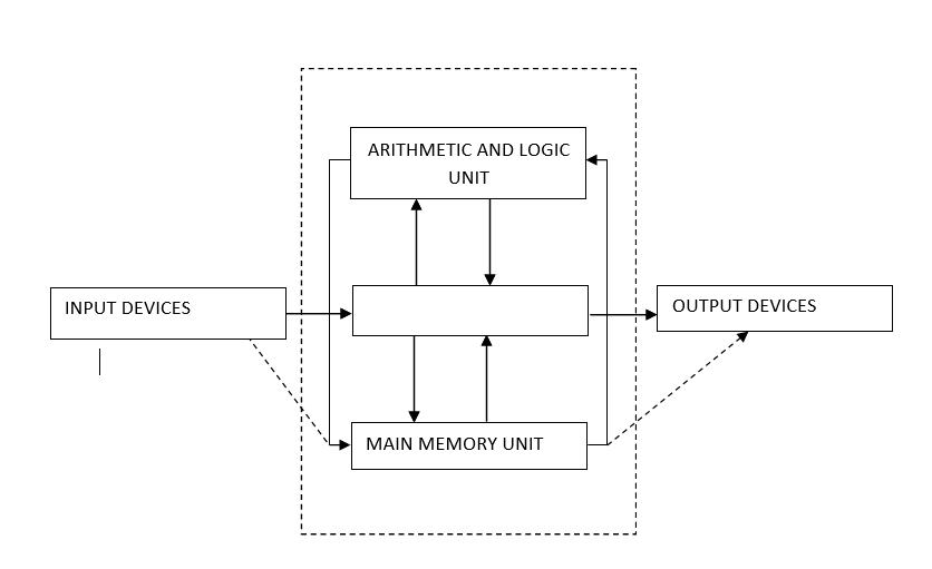
X is the control unit.
- Fetches the next instruction from memory.
- Decodes the instruction.
- Issues control signals to the ALU and registers.
- Coordinates reads/writes and transfers through the buses.
- Sequences instruction execution, updates control flow and handles interrupt requests.
- 110001₂ = 49; 111₂ = 7. Their difference is 42 = 101010₂.
- 111101₂ = 61, 11011₂ = 27, 1001₂ = 9; sum = 97 = 1100001₂.
- Using four bits: 7 = 0111 and 3 = 0011. Complement 0011 to 1100. Add 0111 + 1100 = 1 0011; add the end-around carry: 0011 + 1 = 0100₂ = 4.
- 1011₂ × 110₂ = 11 × 6 = 66 = 1000010₂. Binary partial products: 000000 + 010110 + 101100 = 1000010.
- 11₂ + 11₂ = 3 + 3 = 6 = 110₂.
Question 12
Answer
- The processor recognises an enabled interrupt and completes the appropriate current instruction boundary.
- It saves the program counter, status and necessary registers.
- It identifies the interrupt source/vector and branches to its handler.
- The handler services the device, clears/acknowledges the request and restores the saved context.
- A return-from-interrupt resumes the interrupted program.

P is an uninterruptible power supply (UPS).
- Supplies stored battery power during an outage.
- Allows time to save work and shut down safely.
- Provides surge protection within its design limits.
- Conditions voltage or regulates it where the UPS model supports this.
- Maintains power during short interruptions and transfers; available runtime depends on load and battery capacity.
Question 13
Answer

Let N = (A+B)′ and M = C′. The output is X = (NM)′M = (N′+M′)M = N′M = (A+B)C′ = AC′+BC′.
| A \ BC | 00 | 01 | 11 | 10 |
|---|---|---|---|---|
| 0 | 0 | 0 | 0 | 1 |
| 1 | 1 | 0 | 0 | 1 |
Group the two cells in the A = 1 row at BC = 00 and 10 (wraparound): AC′. Group the two cells in BC = 10: BC′. Thus X = Σm(2,4,6).
- Cache serves repeatedly used instructions/data with lower latency than main memory.
- Temporal and spatial locality improve the hit rate and reduce average memory-access time.
- It reduces repeated traffic to slower main memory and keeps the processor supplied with data.
- One hexadecimal digit represents four binary bits, so long bit patterns are compact.
- Bytes align neatly into pairs of hexadecimal digits, making addresses and masks easier to read than binary.
Question 14
Answer
- Check motherboard/CPU documentation for RAM generation, maximum capacity and compatible modules.
- Back up work, shut down the computer and disconnect power.
- Use antistatic precautions and open the case as documented.
- Release the retaining clips and remove any module being replaced.
- Align the new module’s notch, seat it fully and secure its clips; follow the supported channel arrangement.
- Close the case, reconnect, confirm recognised capacity in firmware/OS and run a memory check.
- Programmed I/O: the CPU polls the device and executes instructions to move data.
- DMA: after CPU setup, a controller transfers blocks directly between the device and memory and reports completion.
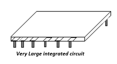
VLSI is associated with fourth-generation computers.
- Microprocessors integrate CPU functions into a chip.
- Computers became smaller and more portable.
- Low power consumption and reduced heat compared with earlier discrete designs.
- Greater reliability due to fewer physical connections.
- Higher processing capability and lower mass-production cost enabled personal computers.